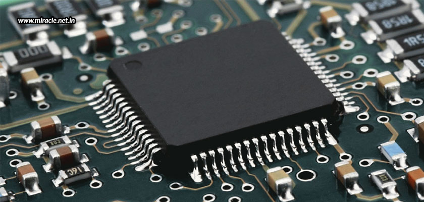
With the modern age of increasing usage of electronic products, PCB remains the most integral part, supporting the electronic components and providing electrical connections between them. The Surface Mount Technology is becoming more popular in developing PCBs, transforming the concept of traditional electronic circuit assembly to build miniature lightweight PCBs. Let’s learn in detail the basic process of Surface Mount Technology.
Step 1 – Printing
A solder paste printing press that is located at the end of the production line is used to print solder paste or patch adhesive onto the circuit board’s solder pad, in order to prepare the components for welding.
Step 2 – Adhesive dispensing
A glue dispenser that is mainly used for precise spot injection of glue paint and other liquids to the precise position of each product is used to drop the glue on the fixed position of the PCB, and fix the components to the board when wave solder is used.
Step 3 – Component placement
With the right amount of solder paste applied, every component is then picked from its packaging using a vacuum or gripper nozzle, checked by the vision system, and placed in the programmed location at high speed. In this way, every component is carefully placed on the board
Step 4 – Automated Optical Inspection
Once the components are placed, it is important to verify that no mistakes have been made, and that all the parts are correctly placed. This requires an AOI machine that can check for component presence, type/value, and polarity.
Step 5 – Reflow soldering
After all the checks are made, the PCB is moved into the reflow soldering machine, where all the electrical solder connections are formed between the components and PCB, by heating the assembly to a sufficient temperature. Here, it is important to ensure that the solder joints are acceptable, without damaging the parts or assembly due to excessive heat.
Step 6 – Automated Optical Inspection
Inspection after soldering is important again to ensure correct solder joint quality, with no mistakes. Poor connections, lack of connections, shorts, and misplaced components should be checked for.
Step 7 – Conformal coating
This step involved a thin polymeric film that conforms to the contours of a PCB to protect the components, typically applied at 25-250 micrometers thickness, acting as protection against moisture, dust, temperature extremes, and chemicals. All in all, conformal coating acts as a protection for the board.
Step 8 – Final inspection
A final inspection is now required to test the PCB for functionality. The tests conducted will simulate the normal circumstances in which the PCB will operate. As the testers monitor the PCB’s electrical characteristics, power and simulated signals run through the PCB.
Step 9 – Washing and drying
Once the entire PCB is built and tested well, it is finally washed and dried before being packed and shipped for delivery.
Once all these procedures are completed thoroughly, you can rest assured that the product you’re receiving is the finest quality PCB assembly. One manufacturer who can bring to you such an exceptional PCB assembly from India is Miracle Electronics, not only for Surface Mount Technology PCBs, but μBGA PCB assemblies too.


